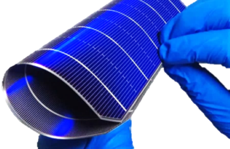
Longi develops flexible heterojunction solar cell with 26.06% efficiency
The Chinese module manufacturer led an international research team seeking silicon material savings and efficiency gains in the development of heterojunction PV devices. The cell achieved a certified power conversion efficiency of 26.06% with a thickness of 57 μm, with Germany’s Institute for Solar Energy Research confirming the result.
Researchers keep pushing the limits of silicon solar cell technology in a quest to use less material in thinner and lighter cells without sacrificing efficiency or durability.
Now, a team led by researchers from Chinese vertically integrated module manufacturer Longi has developed processes to fabricate high-efficiency heterojunction (HJT) solar cells while reportedly avoiding the fragility and lower efficiency results seen in earlier attempts to produce thinner cells.
In the study “Flexible silicon solar cells with high power-to-weight ratios,” published in Nature, the scientists said the new cell ranges in thickness from 57 μm to 125 μm and is made using M6 wafers with an area of 274.4 cm2.
The wafer thinning not only lowers the weight and cost but also facilitates charge migration and separation, noted the research team.
“The flexible and thin profile of these solar cells opens up new opportunities for incorporating solar energy generation into various aspects of daily life and industry, including portable electronics, building integrated PV, transportation, space applications, and emerging technologies with unconventional surfaces or structures,” Xixiang Xu, Longi R&D team leader and corresponding author, told PV magazine.
The team developed its own control and regulation system to enable a continuous low-damage-plasma chemical vapor deposition (CVD) process to prevent epitaxy and maintain surface uniformity. It is a modification of the conventional step-by-step, non-continuous CVD process for passivation, noted the researchers.
In addition, they implemented a “self-restoring nanocrystalline sowing and vertical growth process for the doped contacts” in a high-frequency plasma-enhanced CVD (PECVD) process, which enabled growing “high-quality n-type and p-type carrier selective contacts” for the hole transport layer and electron transport layers.
Another innovation was to use contact-free laser transfer printing to deposit low-shading grid lines. For the transparent conducting oxide (TCO) layers, they opted for cerium-doped indium oxide (ICO) and a low-damage reactive plasma deposition (RPD) process.
The team deposited ICO as the TCO coating using a low-damage reactive plasma deposition method, which they said “produced superior electrical performance, including much lower resistivity (2.7 × 10⁻⁴ Ω cm) and higher carrier mobility (83.1 cm V−1 s −1), when compared to those of the magnetron sputtering-derived indium tin oxide reported elsewhere”, adding that the process “played a decisive role in subsequent stability improvement.”
The cell achieved a certified power conversion efficiency of 26.06% with a thickness of 57 μm, a value of 26.56% with a thickness of 106 μm, and a maximum efficiency of 26.81% with a thickness of 125 μm. The 57 μm solar cell also had the highest power-to-weight ratio (1.9 W g−1) and open-circuit voltage (761 mV).
The results were validated by Germany’s Institute for Solar Energy Research in Hamelin.
The scientists were also able to reduce optical loss by optimizing the configuration of grid lines using “industry-compatible contact-free” laser transfer printing technology. “The finger width could be reduced from 40 μm (typical screen printing) to 18 μm, with the shading area controlled to less than 2%,” they noted.
The devices were tested for potential-induced degradation and light-induced degradation, according to the paper. “This technological progress provides a practical basis for the commercialization of flexible, lightweight, low-cost and highly efficient solar cells, and the ability to bend or roll up crystalline silicon solar cells for travel is anticipated,” concluded the team.
The team included researchers from Jiangsu University of Science and Technology and Curtin University.
Source : pv-magazine.com